General Diamond Properties
Specifications and qualities of diamond
HardnessTensile Strength
Compressive Strength
Fracture Strength
Sound Velocity
Density
Young’s Modulus
Poisson’s Ratio
Atomic Density
Thermal Expansion Coefficient
Thermal Conductivity
Thermal Shock Parameter
Coefficient of Friction
Derbye Temperature
Optical Index of Refraction
Optical Transmissivity Range
Emissivity
Optical Absorption Coefficient
Loss Tangent at 40 Hz
Loss Tangent at 140 GHz
Dielectric Constant
Dielectric Strength
Electron Mobility
Hole Mobility
Electron Saturated Velocity
Hole Saturated Velocity
Work Function
Bandgap
Resistivity
10,000 kg/mm²>1.2 Gpa
>110 Gpa
400–800 MPa at <1 mm thickness
18,000 m/sec
3.52 g/cm³
1200 GPa
0.2
1.77 x 10²³ atoms/cm³
1.1–5.0 (300-1300K) ppm/K
10–20 W/cm-K
30,000,000 W/m
0.05 (dry)
2,200 K
2.41 (at 591 nm)
225 nm to far IR
0.02–0.03 at 10 microns
0.05–0.3 at 10 microns
0.0006
<10-5
5.7
10,000,000 V/cm
2,200 cm²/V-sec
1,600 cm²/V-sec
27,000,000 cm/sec
10,000,000 cm/sec
small and negative on [111] surface
5.45 eV
1013–1016 Ohm-cm
Lab-grown gem diamonds
Creating artisan lab-grown gem diamonds for the jewelry industry is one significant application for Seki Diamond systems.  Notably, CVD diamonds produced by our systems can match or exceed the quality and characteristics of natural diamonds — at much lower cost.
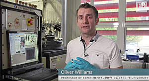
In this video you can see diamonds being grown in the lab on a Seki Diamond system at Cardiff University in the UK.
The many unique advantages of diamond
At 10 on the Mohs scale diamond is four times harder than corundum such as sapphire and ruby. Diamond is highly resistant to scratching and abrasion. It is also chemically inert and resistant to extremely corrosive, radioactive, high temperature environments.
Diamond’s transmission range exceeds that of all traditional IR window materials.
Optically, diamond has the widest transmission band of all known materials, from 220nm to over 50µm, covering UV, visible, infrared, terahertz, and microwave spectral ranges.
With a thermal conductivity of 2000 W/mK diamond exceeds copper by a factor of five while also being electrically insulating.
Its large electronic bandgap of 5.45 eV allows diamond to withstand high electric fields and to be used in hazardous and radiation intense environments.
High intrinsic electron and hole mobility allows electronic charges to travel through the diamond structure with relative ease, which is ideal for high-frequency electronics.
Seki Diamond Systems provides a broad selection of systems for producing synthetic diamonds and diamond films for a spectrum of applications.
-

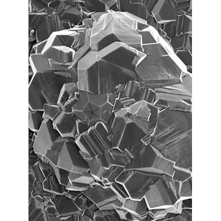
SEM of CVD diamond film grown on Seki Diamond systems at the Melbourne Centre for Nanofabrication
-

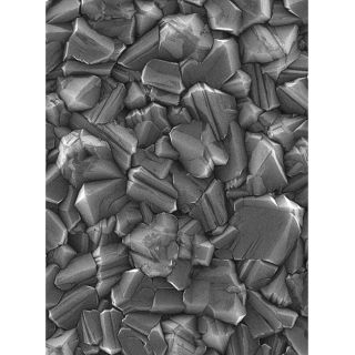
SEM of microcrystalline diamond film, courtesy of Oliver Williams, Cardiff Univ.
-

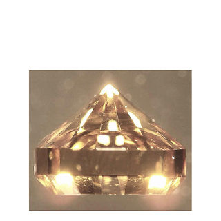
Brilliant cut single-crystal CVD diamond, about 2.5mm high, grown in about 1 day at the Carnegie Institution's Geophysical Laboratory, Washington, D.C.

