Microwave Plasma CVD Systems
from Seki Diamond
A range of systems — entry-level R&D to full production applications
Seki Diamond Systems has long been the world’s leading supplier of microwave plasma CVD diamond systems. Since acquiring ASteX’s technology in 1999, Seki Diamond has enhanced and expanded the product line and delivered hundreds of advanced diamond deposition systems worldwide. Seki Diamond now offers the industry’s broadest selection of standard and custom systems and process solutions for diamond and advanced carbon material synthesis, serving a spectrum of applications.
Seki Diamond systems deliver the highest quality microwave plasma CVD diamond films and highest growth rates available in the industry. They are respected for their exceptional reliability, process flexibility, repeatability and vacuum integrity, giving superior performance even for the most demanding applications.
Number one choice of the world’s leading diamond researchers

Raman spectrum shows the purity of a Seki Diamond CVD diamond film
Diamond scientists consistently choose Seki Diamond systems, to shorten their process development times on microwave plasma CVD diamond and also to leverage the consistency with other diamond specialists and their published research worldwide. Seki Diamond systems are presently in use at most of the world’s leading research centers, including Carnegie, NRL, CEA Saclay, Hasselt, UCL, CNRS, U. Munich, MSU, Vanderbilt, AIST NIMS, NCSU, UCSB, Aston, Cardiff, Stanford, Monash, Melbourne, Harvard, Wisconsin, Texas Tech, Louisville, Waterloo, MIT and many more…
Seki Diamond now has the world’s largest installed base of diamond R&D systems, with more than 80% share of market at university, government and corporate labs — as well as the largest base of commercial microwave CVD systems producing gems, tools and electronic products.
Major Seki Diamond advantages
- High-purity diamond
- High growth rate
- Non-contamination
- Precise doping control
- Excellent process stability & repeatability
- High reliability
- Wide-range process control
Commitment to authenticity
Seki Diamond Systems’ Microwave Plasma CVD (MP-CVD) system hardware, software and support are trusted by the world’s most demanding research labs and gem production foundries. Many companies have attempted to copy Seki Diamond MP-CVD systems without success. All authentic Seki Diamond Systems MP-CVD systems are designed and manufactured in Japan to exacting requirements, ensuring the safest, most reliable, and highest performing MP-CVD platforms in the world.
Seki Diamond Systems does not license its proprietary software and hardware designs to third parties. Any third party claiming to offer a copy or licensed version of the Seki Diamond Systems MP-CVD platform should be dismissed and treated as potentially fraudulent. Don’t be fooled by low performance and unreliable counterfeits. Accept nothing less than authentic Seki Diamond Systems platforms, replacement parts and support!
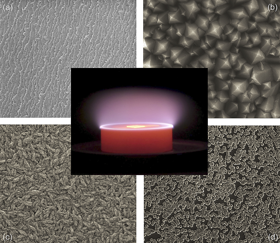
An image of microwave plasma-enhanced chemical vapor deposition diamond film growth (center)1 and scanning electron micrographs of (a) homoepitaxial diamond surface,2 (b) polycrystalline diamond surface,3 (c) ultrananocrystalline diamond surface,4 and (d) B-doped diamond microparticles.5 Courtesy MRS Bulletin, Vol 39, June 2014
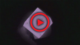
CVD diamond growth in time-lapse video — grown on a Seki Diamond system at the Melbourne Center for Nanofabrication
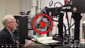
Growing synthetic CVD diamond: Russell J. Hemley, director of the Geophysical Laboratory at the Carnegie Institution for Science, Washington, DC
References for MRS Bulletin images above:
1. G. Bogdan, K. De Corte, W. Deferme, K. Haenen, M. Nesládek, Phys. Status Solidi A 203, 3063 (2006).
2. K. Haenen, A. Lazea, M. Nesládek, S. Koizumi, Phys. Status Solidi (Rapid Research Letters) 3, 208 (2009).
3. A. Lazea, V. Mortet, J. D’Haen, P. Geithner, J. Ristein, M. D’Olieslaeger, K. Haenen, Chem. Phys. Lett. 454, 310 (2008).
4. O.A. Williams, M. Daenen, J. D’Haen, K. Haenen, M. Nesládek, D.M. Gruen, Diam. Relat. Mater. 15, 654 (2006).
5. S. Heyer, W. Janssen, S. Turner, Y.-G. Lu, W.S. Yeap, J. Verbeeck, K. Haenen, A. Krueger, ACS Nano (2014), doi 10.1021/nn500573x.
-

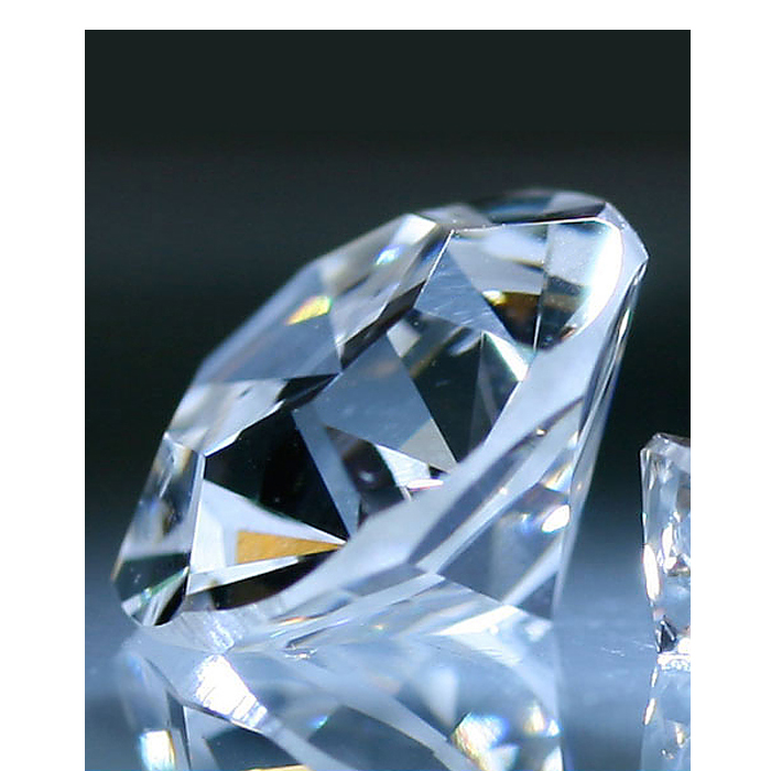
CVD diamond, Carnegie Institution
-
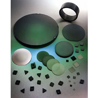
Diamond-coated wafers, inserts, films
-
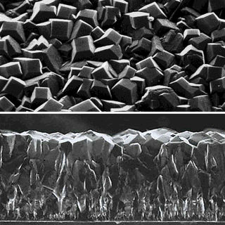
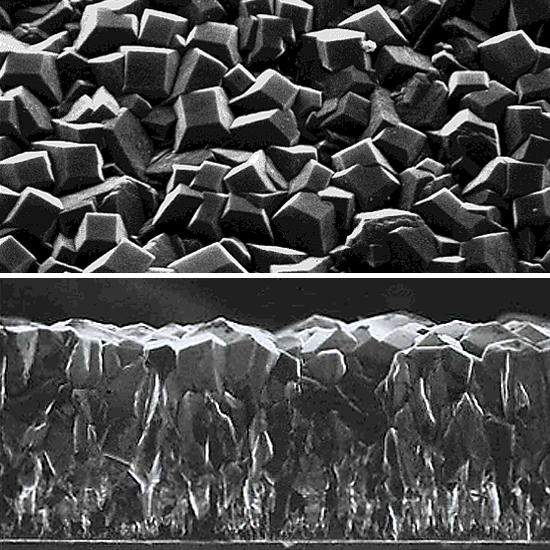
Microcrystalline diamond film. top and cross section. Courtesy of Paul W. May, U. of Bristol.
-
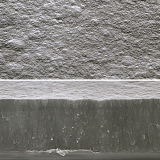
Nanocrystalline diamond film. top and cross section. Courtesy of Paul W. May, U. of Bristol.